![](/_images/main/main_visual_001.jpg)
![](/_images/main/main_visual_03.jpg)
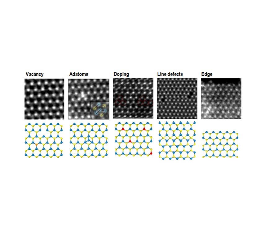
Defects of 2D Crystals and its Applications
![](/_images/main/main_visual_02.jpg)
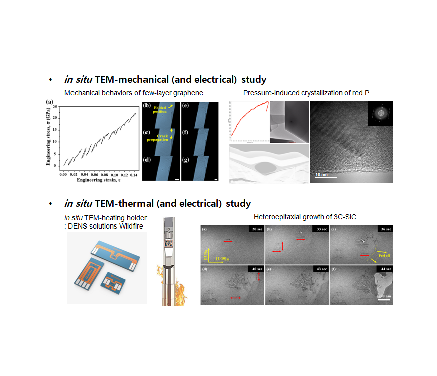
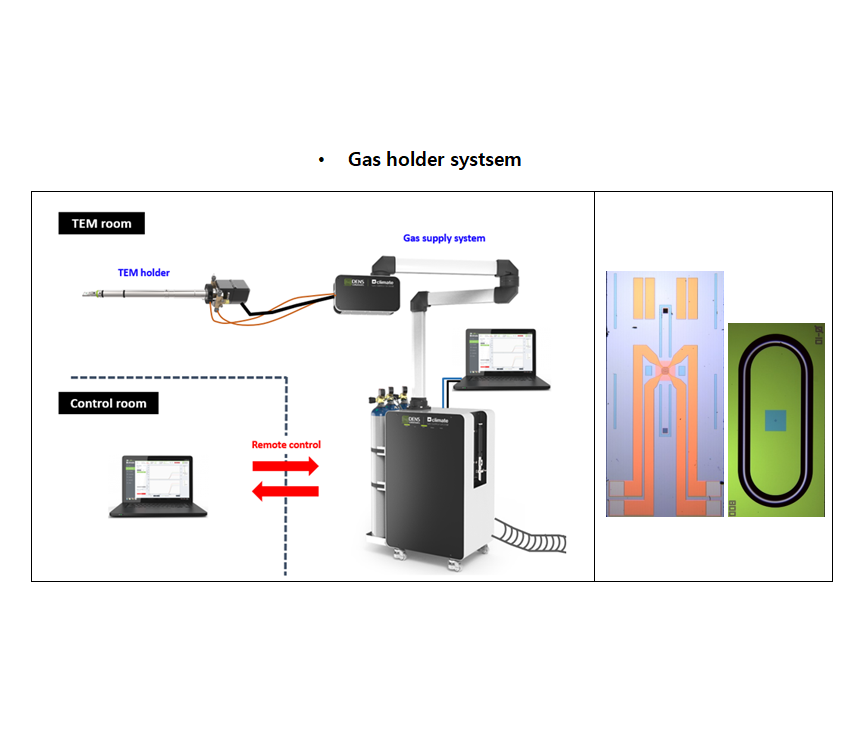
In Situ TEM Experiments at Nano and Atomic Scale
![](/_images/main/main_visual_05.jpg)
Interfaces of Advanced Materials
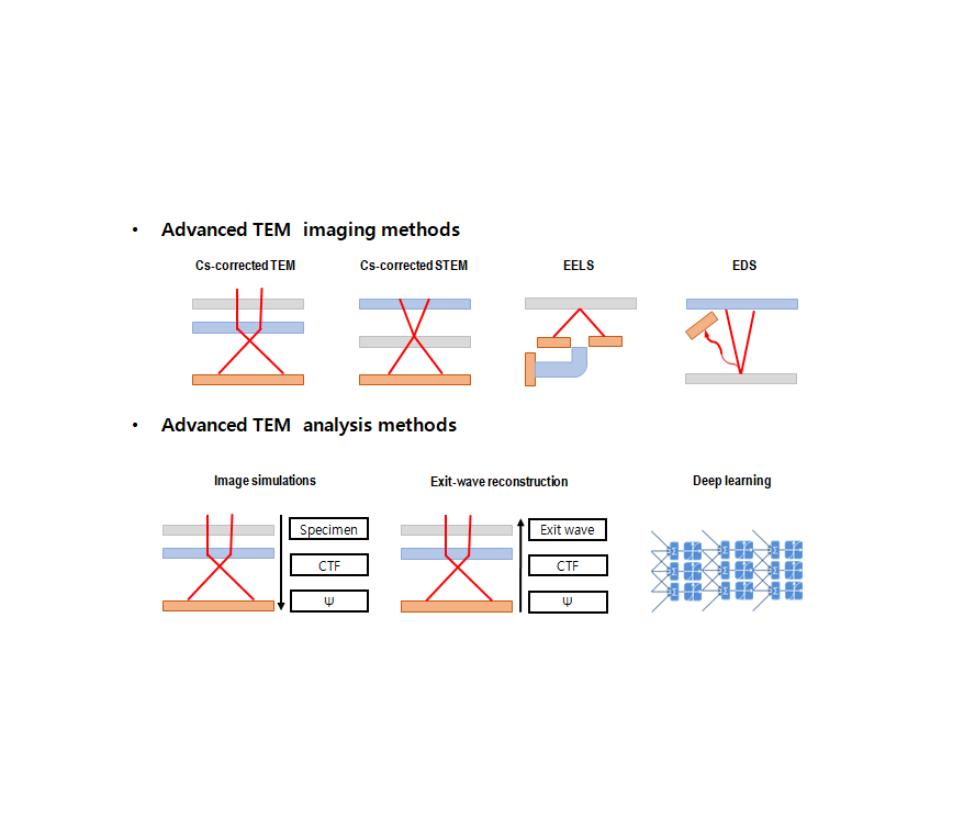
![](/_images/main/main_visual_04.jpg)
We characterize the structure and EELS/EDS spectroscopy of new materials with aberration-corrected TEM/STEM at the atomic scale.
The unique intrinsic and extrinsic defects of low-dimensional materials bring extraordinary electrical, optical, and magnetic properties.
Investigation on deformation and phase transformation of materials with external stimuli including mechanical, thermal, and electrical inputs is significant for design, manipulation and maintenance of the materials.
Many reactions in real-life occur in the gaseous state, including materials nucleation and growth, interfacial interaction, energy conversion, and catalytic reactions.
[2024/05] Teacher's day
[2024/04] Lab Picture Day
[2024/03] ASEM Lab Workshop